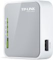
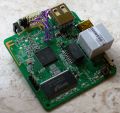
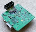
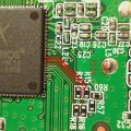
TP-LINK TL-MR3020 v1.x
TP-LINK TL-MR3020 v1.x
Availability: now
FCC approval date: 21 February 2012
(Est.) release date: 13 January 2012
UPC: 845973051709 (UPC DB, On eBay)
EAN: 6935364051709 (UPC DB, On eBay)
Country of manuf.: China
Amazon image
ASIN
B00634PLTW (![]() , On Amazon, On CCC, multiple uses)
, On Amazon, On CCC, multiple uses)
multiple revisions of this device, use caution
Type: mobile router
FCC ID: TE7MR3020
PCB ID: 2050500194
Power: 5 VDC, 1 A
Connector type: USB Female Mini-B
CPU1: Atheros AR9331
FLA1: 4 MiB4,194,304 B <br />32,768 Kib <br />4,096 KiB <br />32 Mib <br />0.00391 GiB <br /> (Spansion S25FL032PIF)
RAM1: 32 MiB33,554,432 B <br />262,144 Kib <br />32,768 KiB <br />256 Mib <br />0.0313 GiB <br /> (Winbond W9425G6JH-6)
Expansion IFs: USB 2.0
USB ports: 1
WI1 chip1: Atheros AR9331
WI1 802dot11 protocols: bgn
WI1 MIMO config: 1x1:1
WI1 antenna connector: none
ETH chip1: Atheros AR9331
LAN speed: 100M
LAN ports: 1
bgn
Flags: 3G capable
802dot11 OUI: none specified
| CPU1 brand | WI1 chip1 brand | WI1 chip2 brand | |
|---|---|---|---|
| TP-LINK TL-MR3020 v1.x | Atheros | Atheros | |
| TP-LINK TL-MR3020 v3.x | MediaTek | MediaTek |
For a list of all currently documented Atheros (QCA) chipsets with specifications, see Atheros.
Portable 3G Wireless N Router
- TP-LINK TL-MR3020 v3.x (v3/v3.20)
- CPU: MediaTek MT7628NN @575MHz WiSoC
- Flash: GigaDevice GD25Q64BSIG (8MB)
- RAM: Zentel A3R12E40DBF-8E (64MB)
- WLAN: 802.11bgn 2T2R (2.4GHz)
- LAN: 1x FE, USB: 1x USB 2.0 port
- PCB ID: 2050500974
Notes on JTAG
The EJTAG interface AR9331 is different from the ones on most chips:
- First of all, the Jtag pins are multiplexed with GPIOs, GPIO11 must be pull high to bootstrap the debug interface.
- Pressing the SW2 switch while powering on the unit should take care of this as it is connected to GPIO11.
- The second problem is that U-Boot will disable EJTAG, even if it was enabled by pulling GPIO11 high during power up.
- To workaround this, a jumper can be added between the CS pin on the flash and CPU.
- And last problem is that TP-Link does not provide test points, pads or pins for the Jtag interface.
OpenOCD
This sequence will be needed to initiate PLL and RAM:
| • PLL / RAM • >> |
|---|
        #pll initialization
        mww 0xb8050008 0x00018004
        mww 0xb8050004 0x00000352
        mww 0xb8050000 0x40818000
        mww 0xb8050010 0x001003e8
        mww 0xb8050000 0x00818000
        mww 0xb8050008 0x00008000
        sleep 1
        # Setup DDR1 config and flash mapping
        mww 0xb8000000 0x7fbc8cd0
        mww 0xb8000004 0x9dd0e6a8

        mww 0xb8000010 0x8
        mww 0xb8000008 0x133
        mww 0xb8000010 0x1
        mww 0xb800000c 0x2
        mww 0xb8000010 0x2
        mww 0xb8000010 0x8
        mww 0xb8000008 0x33
        mww 0xb8000010 0x1
        mww 0xb8000014 0x4186
        mww 0xb800001c 0x8
        mww 0xb8000020 0x9
        mww 0xb8000018 0xff

        #UART
        mww 0xb8020004 0x4388
        mww 0xb8020008 0xc2000

        #GPIO
        mww 0xb8040028 0x48002
|
Images


